EPFL Team
 | Ionescu Mihai Adrian |
 | Kis Andras |
Low-power Vector-by-matrix Multiplication Processor Based on a 2D FeFET
Modern processors perform many functions needed for the operation of our electronic devices. This flexibility was initially enabled by the separation of processing and memory units in the von-Neumann architecture. However, current data-driven applications are imposing energy constraints on edge devices due to intensive use of vector matrix-multiplications and access to memory in deep neural networks 1. This can be mitigated by performing computation directly in the memories' physical layer through the combination of Kirchhoff's and Ohm's laws. Such in-memory processing can benefit calculation-intensive applications such as solving linear system equations, linear regression, image/signal processing and compression, as well as in artificial neural networks (ANN).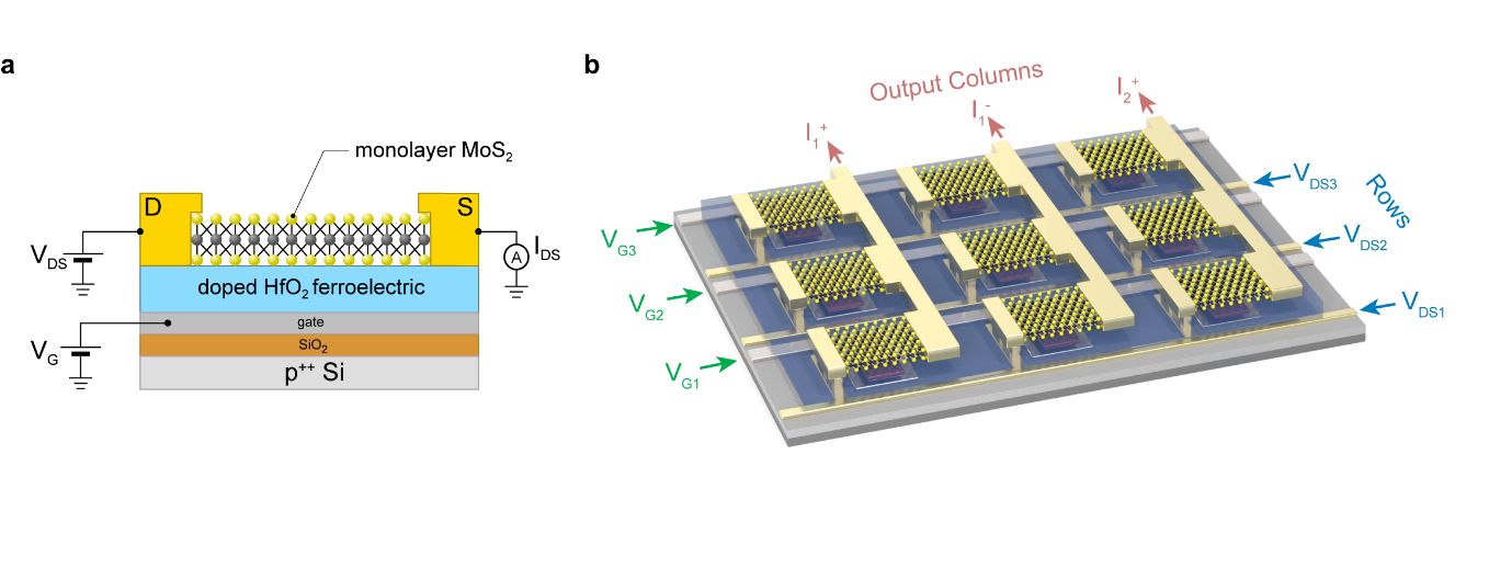
The strong electrostatic sensitivity of two-dimensional (2D) materials present a promising pathway towards reconfigurable and low-power neuromorphic hardware. Monolayer transition metal dichalcogenides (TMDCs), such as MoS2 have been attracting great attention due to their potential to extend Moore's law in advanced technological nodes 2-5. Moreover, their use in emerging memory devices has also been widely reported. 2D materials such as MoS2 as especially interesting for the realization of memories in the form of floating-gate field-effect transistors (FGFETs) and FeFETs. At EPFL, the Kis group has recently realized logic-in-memory based circuits based on MOCVD-grown MoS2 FGFET devices6 as well as simple artificial neural networks 7.
For this project, Ionescu and Kis groups will combine their respective expertise in low-power FETs with ferroelectric gates (Ionescu) and 2D materials and their processing (Kis) to realize MoS2 FeFETs in a scalable fabrication approach and evaluate the memory device performance with the perspective of applications in neural networks. Next-generation 2D FeFET memory devices (Figure 1) will be fabricated on a wafer scale by combining HfO2 ferroelectric layers with wafer-scale, MOCVD-grown monolayer MoS2 at the BEOL. W High-quality, wafer scale and continuous monolayer MoS2 will be grown on sapphire at optimal conditions and transferred onto the gate stack. Electrical contacts to MoS2 will then be realized and the entire 2D part of the process (transfer, patterning) will be carried out at less than 200 °C. MoS2 FeFET devices will be electrically characterized and the ability to set the multilevel behaviour with the programming pulses verified. Program level stability and retention times will be measured to establish feasible programming resolution. Arrays of FeFET devices will be realized and characterized by taking advantage of the high quality and homogeneity of the MoS2 film. Arrays will be benchmarked in terms of yield, device-device variation, power consumption, programming linearity, stability, retention and power requirements.
1. Xu, X. et al. Scaling for edge inference of deep neural networks. Nat. Electron. 1, 216-222 (2018).
2. Radisavljevic, B., Radenovic, A., Brivio, J., Giacometti, V. & Kis, A. Single-layer MoS2 transistors. Nat. Nanotechnol. 6, 147-150 (2011).
3. Agarwal, T. kumar et al. Material-Device-Circuit Co-optimization of 2D Material based FETs for Ultra-Scaled Technology Nodes. Sci. Rep. 7, 5016 (2017).
4. Smets, Q. et al. Ultra-scaled MOCVD MoS2 MOSFETs with 42nm contact pitch and 250µA/µm drain current. in 2019 IEEE International Electron Devices Meeting (IEDM) 23.2.1-23.2.4 (2019). doi:10.1109/IEDM19573.2019.8993650.
5. Iannaccone, G., Bonaccorso, F., Colombo, L. & Fiori, G. Quantum engineering of transistors based on 2D materials heterostructures. Nat. Nanotechnol. 13, 183-191 (2018).
6. Migliato Marega, G. et al. Logic-in-memory based on an atomically thin semiconductor. Nature 587, 72-77 (2020).
7. Migliato Marega, G. et al. Low-Power Artificial Neural Network Perceptron Based on Monolayer MoS2. ACS Nano 16, 3684-3694 (2022).